
Design Progress | Week 8
- Oct 15, 2025
- 2 min read
Dates: 10/08/25 - 10/14/25
This week, I began using new components for the first time in testing systems, namely the Polulu U3V40F5 5V Boost Converter for driving stable 5V from the 3.7V LiPO battery, and the CD74HC4051E 8:1 ADC Multiplexer for controlling the 8 IR sensors with the limited 3 ADCs located on the pico 2. I was successfully able to design a system which controls multiple IR sensors at once and is portable (i.e. all powered by the LiPO battery).
First, I needed to solder some pin headers to the boost converter, and connector wires to the loose wires attached to the 5 pin JST connectors for the IR sensors. Note that this current system only makes use of 5 IR sensors as we are awaiting more in the mail, but very little needs to change in this system to accommodate the additional sensors.

Then, after soldering all 25 JST wire connections, I placed them into the circuit as follows:
The LiPO battery is being driven to the breadboard's top (+) and (-) buses
The Boost Converter VIN and GND are connected to aformentioned buses
Boost Converter EN tied to VIN (always enabled) and VOUT sent to bottom (+) bus (common GND)
Each sensor has two GND and two VCC connections, each are assigned to bottom buses
Remaining 1 JST connection for each sensor assigned to specific signal input of multiplexer
Multiplexer powered by 3V3 on pico (VCC) and tied to common ground.
S0, S1, S2 for selecting active Multiplexer channel assigned to Pico GPIO 2, 3, 4
Mult VEE also tied to GND, and common output (Z) assigned to ADC0 (GPIO26).

Below is the front facing view of the system's sensors. Note the orientation is as follows:
Top Sensor - Pointed Forward
Middle Left Sensor - Pointed Left
Middle Right Sensor - Pointed Right
Bottom Left Sensor - Pointed Down and Slightly Left
Bottom Right Sensor - Pointed Down and Slightly Right

And the back facing view of the sensors, connected to the aforementioned system containing the boost converter, multiplexer, and pico.

The code remained largely the same, however there was new logic included to account for the Multiplexer based selection of the active sensor, rather than iterating through the ADC pins.
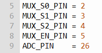
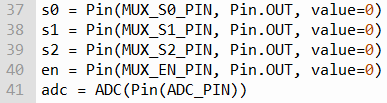
Below, the multiplexer signal pins and enable pins are selected to be Pico GPIO pins 2, 3, 4, and 5 respectively, with the active ADC pin being selected as GPIO26 (ADC0). Then, signal variables were were used to assign these selections to output pins with a starting value of 0 (enabled).
Then a new function was defined to iterate between the three select pins s0, s1, and s2. To do this, I used the SHR binary operation to check each binary digit representation of the active channel number (i.e. channel 3 is 011), and AND it against 1 to retain only the LSB. This allows for the separation of the composition of said binary representation to individually control each of the set pins accordingly.

Then, the operational loop changes from iterating throught the 3 ADCs to the length of SENSOR_CHANNELS for each sensor.

Below is a video demo of this week's progress.


Comments